UTEP Lab Pioneers Electromagnetics and Photonics
Last Updated on December 11, 2017 at 12:00 AM
Originally published December 11, 2017
By Lauren Macias-Cervantes
UTEP Communications
Ask anyone in Raymond Rumpf’s EM Lab what they do and they’ll tell you they are doing what most would consider impossible. Failure is common in their work in electromagnetics and photonics, but it is revolutionizing engineering and science as we know it.
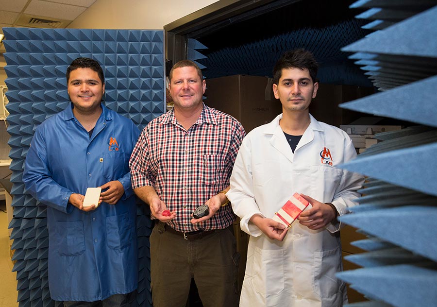
Rumpf, Ph.D., Schellenger Professor in the Department of Electrical and Computer Engineering and Director of the EM Lab at The University of Texas at El Paso, is a pioneer in 3-D printing of high-frequency circuits and electromagnetic devices. His mission at UTEP is to develop revolutionary technologies that are enabled by 3-D printing.
He founded the EM Lab in 2011 and his team has already delivered an array of significant breakthroughs, including inventing at least two new electromagnetic phenomena. Other accomplishments include creating the world's highest power frequency selective surface, the world's most broadband all-dielectric filter, the world's tightest bend of an unguided optical beam, the world’s thinnest all-dielectric antenna, and spatially variant anisotropic metamaterials (SVAMs).
Most recently, the team’s work has resulted in a new patent for anisotropic metamaterials for electromagnetic compatibility, and a three-year grant from the National Science Foundation.
“In one area, we’ve invented a new electromagnetic phenomenon that lets us change the shape of the electromagnetic fields around devices,” Rumpf said.
The discovery related to the patent allows the researchers to sculpt electromagnetic fields like clay. One of the applications of their invention could be used in cell phones. The team is presently working with cell phone antennae.
“There’s a lot of stuff crammed really close, creating a terrible electromagnetic environment inside cell phones,” Rumpf explained. “It’s not so much that the antenna is terrible, it’s that it is so close to other metal things, close to other antennae, that it just can’t work very efficiently. Typical antennas in mobile phones are 50 percent efficient or less, so more than half of the energy from your battery is going to heat and being wasted.”
The research toward the patent awarded this fall took years.
“We think we have a rather powerful technology that will help us pack electrical components more closely and sort out the electromagnetic mess this causes,” Rumpf said. “However, there are also new device concepts that this will let us explore.”
Doctoral candidate in electrical engineering Edgar Bustamante is involved in the research.
“The most rewarding part about my research is knowing that it could help mobile devices work dramatically better, and everyone who uses a cell phone can benefit from this,” Bustamante said.
The breakthrough also will give circuits new functionality, Rumpf said. Next, the team will work on proving their discovery in settings other than their 3-D printed model mobile phone.
“I think if we are successful it will revolutionize electromagnetics for sure and that is pretty exciting,” Rumpf added. “It’s a high-risk technology. There is a real chance that something will go wrong. That is a consequence of working on the edge.”
Rumpf’s research team is comprised of highly ambitious engineers. They are all doctoral candidates fueled by the opportunity to explore the unknown and do the impossible.
“Our work is ground breaking and never conceived before,” said Ubaldo Robles, a Ph.D. candidate in electrical and computer engineering. “We are right at the edge of theoretical physics and applied science and sometimes we even drift past that. Most of our concepts haven’t been imagined by scientists before. My role in the EM Lab has made me one of only a handful of people who can design, develop, manufacture and test 3-D-printed electronics in the world.”
Noel Pedro Martinez, another doctoral candidate in electrical engineering, echoes the incredible experience the students are getting by working in the EM Lab.
“The work the EM Lab does is very important for both the students and the university,” he said. “Obviously, for students it provides us with the opportunity to conduct cutting-edge research and acquire some degree of fame and notoriety in our fields of study. Not only do we conduct research that could change the world, but the EM Lab also has all of the capabilities and resources necessary to see the research through from start to finish. Students get training to use high-end machines and industry standard software. For the University, it helps further UTEP’s mission of becoming a top research institution and develop a reputation for producing research that exceeds that of the bigger universities.”
Martinez joined the EM Lab three years ago. His current work involves a new concept called “photon funnels.”
Collecting and concentrating light is an essential process in any system utilizing light. Conventional lenses collect light and concentrate it to a spot, but the concentration spot moves as light rays strike the lens at different angles or different positions. As a result, sensors and detectors lose energy as the light changes.
“Photon funnels are nanoscale 3-D lattices that direct the flow of light using a new optical phenomenon recently invented by the EM Lab,” Martinez explained. “We design the photon funnels using a novel algorithm developed here at the EM Lab that can bend, twist and otherwise spatially vary our lattices without degrading their magical properties. Imagine having to abruptly bend the pattern of a checkerboard, but without changing the size and shape of the squares. Seems impossible, right? But we figured out how to do it and we are the only ones in the world who can.”
The group received a grant for $174,000 from the National Science Foundation during the summer for the research on photon funnels. Rumpf and his EM Lab team are working with Stephen Kuebler, Ph. D., associate professor of chemistry at the University of Central Florida (UCF), and his lab.
“What’s neat about this is that almost all optical devices are limited by refraction, where the angle of the transmitted light depends on the angle of incident light,” Rumpf said. “Our lattices are able to break Snell’s law that describes refraction, allowing us to beat the performance of lenses for collecting light. This seems to violate fundamental physics, but we at the EM Lab do not let fundamental physics get in the way of good ideas. Inside our lattices there is no refraction, it ceases to exist, so we can circumvent the conventional laws of optics that are limiting everybody.”
Using a multidisciplinary approach that combines theory, simulation, fabrication and optical testing, the team will develop fundamental knowledge to enable scientists and engineers to design photon funnels for a myriad of applications.
UTEP is responsible for the design and theory and the UCF team will conduct the fabrication and testing. The benefits to society of the three-year project will include new technologies for imaging, optical detection and sensing, telecommunications, energy harvesting, and relaxed alignment tolerances in photonic systems.
“The most rewarding part about research is the excitement and satisfaction that comes with achieving a new breakthrough,” said electrical engineering doctoral student Cesar Luis Valle. “Much of our time is spent being hopelessly stuck on a problem for what can be long periods of time. Finally being able to solve a problem and reaching that ‘Eureka!’ moment is exhilarating.”
Valle is working on another aspect of the EM Lab’s work that has to do with metamaterials, photonic crystals and 3-D printing.
“I am involved on a patent that contains new photonic crystal technologies and methods,” Valle explained. “Photonic crystals are periodic structures that allow us to manipulate electromagnetic radiation in new ways and are also one of the technologies our group has become famous for. Another aspect of my research involves the use of our nScrypt 3Dn Tabletop hybrid 3-D printer capable of printing multiple types of materials (plastics and conductors) at the same time and engineering new processes that are only achievable with the use of this hybrid 3-D printing technology.”
Gilbert Carranza, a doctoral student in electrical and computer engineering, was highly drawn to the 3-D printing and unconventional technologies the EM Lab regularly explores. Though he has only been a part of the group for a couple of years, his research has already broken barriers. His prior research for the EM Lab involved developing a tool to design truly three-dimensional electronic circuits. 3-D circuits are smaller, lighter, more power efficient, and can be made into shapes not possible with traditional circuit technology.
“I found the first completed version of the 3-D CAD circuit tool I developed to be very rewarding,” Carranza said. “We now have ideas of what three-dimensional circuits might look like in the future. The fact that I am seeing what no one else has ever seen before is amazing to me. It will be even more rewarding when the tool is refined and optimized to produce even more complicated and intricate models and designs.”
The list of accomplishments and ongoing research also includes work on a multiple-input/multiple-output (MIMO) antenna configuration to improve communication devices, and exploring concepts to build and test proof-of-concept asymmetric electromagnetic devices to assess asymmetric behavior that exists at interfaces for Lockheed Martin Aeronautics.
Three other patents are pending related to the work at the EM Lab.
“In the beginning, it was just a bunch of insane ideas that people were shaking their heads at,” Rumpf said. “Over the years, we’ve managed to prove our concepts to a point where people are convinced and are seeing all of the ways the concepts can be used.”
To find out more about the EM Lab, visit it online.