
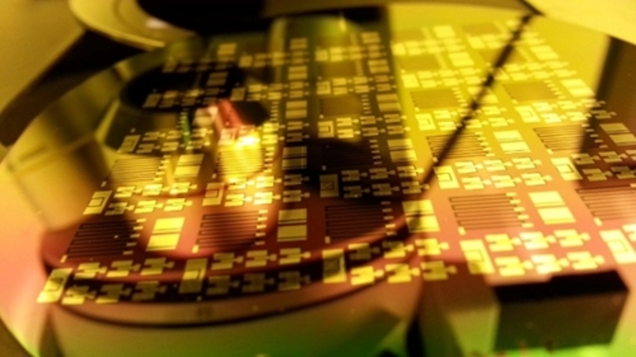
Negative Lithography
Equipment Preparation
Turn-on hot plates and mask aligner UV lamp so they are warmed up when they are needed.
Surface Preparation
Before applying the photoresist, it is important to determine whether the wafers will need to be cleaned. If the surface is free of particles or other types of residues, then it can be considered clean enough for the lithography process. Furthermore, if problems are encountered during the spin coating of the photoresist, then at least a fresh piranha cleaning is recommended. Refer to the cleaning section for detailed cleaning instructions.
After oxidation, the substrate surface should be sufficiently clean if they were stored in a clean container so that no further cleaning is needed. If the wafer has no oxide use nitrogen to remove any potential surface contaminants.
Photoresist Application
Next the wafer is evenly coated with the photoresist. The most popular technique for obtaining a thin, uniform coating of photoresist is by spinning. The substrate is held on a vacuum chuck, while several drops of photoresist dispensed and allowed to spread over the surface. The substrate is accelerated at a high rate to a constant speed, which is maintained for a specific time, depending on the viscosity of the photoresist and the desired thickness of the coating. Note that the photoresist is sensitive to ultra-violet (UV) light and shouldn’t be exposed to it.
The resist thickness depends on the spinner rotation speed (RPMs) according to the following equation,
where k is a spinner constant, p is the resist solids content, and ω is the spinner rotation speed. An adhesion promoter will be necessary if an oxide is present.
Procedure: Adhesion Promoter Application
- Setup the spin-coater to the appropriate recipe #11.
- Center the wafer on the chuck. Use the vacuum in the spin-coater to keep wafer from moving.
- Apply 2ml of HMDS (Hexamethyldisilaxane) on the wafer.
- Press Start.
- Bake the wafer with the HMDS by placing the wafer on the hot plate (HMDS facing up) at 110℃ for 2 minutes.
Procedure: Photoresist Application
- Setup the spin-coater to recipe #14 for a 1.5 um thickness.
- Center the wafer on the chuck.
- Apply 1 mL pipette of AZ5214E photoresist for every inch of diameter length on the wafer.
- Press start.
Procedure: Spin Coater Cleaning
- Remove excess chemical with a wipe.
- Disconnect power, nitrogen and vacuum lines to spin coater.
- Open the lid and pour 150 ml of acetone from the top and collect the acetone from the drain using a beaker.
- Wipe the excess acetone with a wipe.
Soft bake
The photoresist coated wafer is then baked to dry it and improve adhesion to substrate. The time-temperature settings must be sufficient to drive off the solvent without thermally cross-linking the photoresist therefore it is important to use the correct temperature.
- Bake the wafer with freshly spin-coated photoresist by placing the wafer on the hot plate (PR facing up) at 110℃ for 1.5 minutes.
- Remove the wafers and let them cool down for a few seconds.
Alignment and Exposure
In this procedure the mask is aligned with the wafer and the photoresist is selectively exposed to UV light through the mask. This process uses contact printing with manual mask-alignment. This equipment is extremely delicate. Please be careful with it. Follow instructions given by the TA. For additional information refer to the appendix. In negative lithography It is necessary to do an image reversal for the photoresist used in this lab.
Procedure: Alignment and Exposure
- Load the appropriate mask on the mask holder and turn on the vacuum.
- Load the wafer.
- Align the wafer and mask.
- Expose the wafer for 5 seconds, the power should read close to 2.20 mW/cm2.
- Remove the wafer.
Procedure: Image Reversal Bake
- Set the hot plate to 110℃.
- Place the wafer (PR facing up) on the hot plate for 1.5 minutes.
- Remove the wafers and them cool down for a few minutes.
Procedure: Flood Exposure
- Load the appropriate mask on the mask holder and turn on the vacuum.
- Load the wafer.
- Align the wafer and mask.
- Expose the wafer for 95 seconds, the power should read close to 2.20 mW/cm2.
- Remove the wafer.
Development
This process essentially entails removing unwanted resist by way of chemical etching. Development is performed by immersing the wafers in a proprietary developing solution followed by a DI rinse. If the desired pattern is not achieved, the photoresist can be removed and the photolithography process repeated.
The development time is critical so do not leave the wafer in the developer too long. Otherwise small features will be overdeveloped and disappear. It is important to immediately rinse the wafers in DI after the specified time to stop the development process.
Procedure: Development
- Pour developer solution in the petri dish.
- Immerse the wafers in the developer solution for exactly the time specified in the table.
- Immediately rinse in DI for 10 minutes. Not rinsing long enough will lead to the pattern being overdeveloped.
- Dry the wafers with nitrogen.
Procedure: Pattern Check
- Use microscope to determine a good quality of pattern in the windows.
- If the quality is good, proceed to the hard bake procedure.
- If the quality is not good, remove the photoresist and restart from wafer dehydration step.
**Procedure: Photoresist Removal (If quality of lithography is not good)**
- Pour photoresist remover in the petri dish.
- Immerse the wafers in the photoresist remover for the time specified in the table.
- Rinse the wafers in DI for 5 minutes.
- Dry the wafers with nitrogen.
Lift off
This process is the general method of removing photoresist after deposition of a film on a wafer patterned by negative lithography. It takes advantage of the height different between the photoresist and the thin film to simply lift away the photo resist while keeping the patterned film intact.
- Set a hot plate to 200℃.
- Pour AZ400T stripper on a petri dish.
- Place petri dish on the hot plate for a minute or until evaporation becomes visible.
- Immerse the wafer in the solution for 35 minutes.
- Rinse the wafer with DI for a minute. Dry with nitrogen.
Sonic Cleaning
It is possible that during the lift off process some particles will land on the surface of the wafer once more. It will generally be visible to the naked eye, but it is recommended to view under a microscope. If the quality of the lift off is as desired, the sonic cleaning can be skipped.
- Set the sonic sink to 60 ℃.
- Pour DI into the sonic sink until the line is reached.
- Pour acetone into a petri dish, make sure the carefully drop onto the sonic sink so that it remains floating.
- Immerse the wafer in the acetone and sonicate for 7 minutes.
- Carefully remove the petri dish from the sink.
- Pour IPA or Methanol into a different petri dish, carefully drop onto the sonic sink.
- Immerse the wafer in the new petri dish and sonicate for 7 minutes.
- Carefully remove the petri dish from the sonic sink.
- Rinse the wafer with DI for a minute and dry with nitrogen.
Table added for better visual of recipe. Bold is only if oxide layer is present.
Lithography Parameters for 3-inch wafer
|
Process Step |
Parameter |
Value |
|
Wafer Preparation (dehydration) |
Temperature (C) |
110-120 |
|
Time (min) |
2 |
|
|
Adhesion Promoter Application |
Adhesion Type |
HMDS |
|
Volume (mL) |
2 |
|
|
Spinner Recipe |
#11 |
|
|
Speed (RPM) |
7000 |
|
|
Time (sec) |
35 |
|
|
Adhesion Promoter Bake |
Temperature (C) |
110 |
|
Time (min) |
2 |
|
|
Resist Application |
Photoresist Type |
AZ5214E |
|
Volume (mL) |
3 |
|
|
Spinner Recipe |
#14 |
|
|
Speed (RPM) |
6000 |
|
|
Time (sec) |
45 |
|
|
Soft Bake |
Temperature (C) |
110 |
|
Time (min) |
1.5 |
|
|
Exposure |
Power (mW/cm2) |
~2.2 |
|
Time (sec) |
5 |
|
|
Image Reversal Bake |
Temperature (C) |
110 |
|
Time (min) |
1.5 |
|
|
Flood Exposure |
Power (mW/cm2) |
~2.2 |
|
Time (sec) |
95 |
|
|
Development |
Developer Type |
AZ 300MIF |
|
Time (sec) |
55 |
|
|
Lift off |
Temperature (C) |
120 |
|
Stripper Type |
AZ400T |
|
|
Time (min) |
35 |


